How Photonic Integration Is Reshaping Data Center Architecture
Data centers around the world are under more and more pressure to offer working speeds that are exponentially faster while also using less energy and taking up less space. Photonic integration solves these problems by combining many optical parts onto a single chip. This lets data be sent at the speed of light instead of just using electrical signals. Because of this change in architecture, parts need to be made with micron-level accuracy, which is where precision CNC turning has become essential. Photonic modules can work consistently in harsh conditions thanks to high-tolerance housings, alignment fixtures, and temperature management elements made through advanced machining. They are the physical foundation of the next generation of network infrastructure.
Understanding Photonic Integration in Data Centers
What Makes Photonic Integration Different
Copper-based electrical interconnects are used in most traditional data centers. These create a lot of heat and have speed problems when the amount of data increases. Photonic integration adds to or replaces these links with light paths built into small silicon chips. Lasers, modulators, waveguides, and photodetectors are all built into these photonic integrated circuits, which are smaller than a postage stamp but can send terabits per second. Compared to copper alternatives, this technology cuts delay to nanoseconds and energy use by 30 to 50 percent.
The Manufacturing Challenge Behind Optical Components
For photonic modules to work, their housings and fixing structures need to be made to within five microns of accuracy. To keep the signal from getting lost, the threaded metal cases that hold sensitive optical chips must stay circular within 0.002 inches. Parallel turning operations make the cylinder-shaped surfaces that hold fiber-optic connections, and facing operations set up reference lines for aligning the laser. Picking the right material is important. 6061-T6 aluminum is great for high-density optical systems because it is thermally conductive and easy to machine.
Why Precision Manufacturing Matters
Even small changes in the dimensions of the housings of photonic components can seriously damage the signal. If a fiber connection isn't lined up right, light will scatter, which will mess up data transfer. Laser modules' wavelengths move when heat sinks that aren't made well expand when they get hot. We've seen procurement teams change the requirements for important optical interfaces from the usual Ra 3.2μm surface finishes to Ra 0.8μm or smaller, because they know that surface roughness has a direct effect on how well they couple. Because of this rise in quality, industrial relationships with proven skills are now required rather than optional.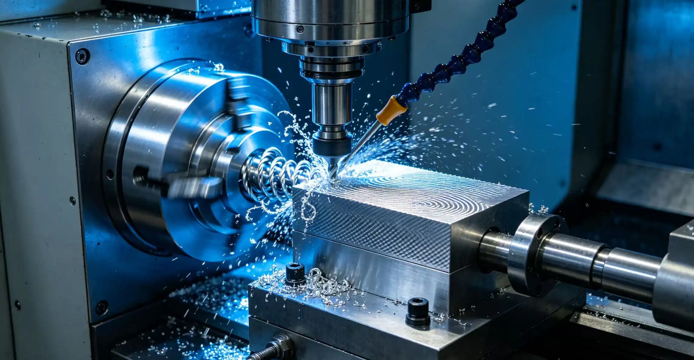
From Traditional Data Center Architectures to Photonic-Integrated Systems
Limitations Driving the Architectural Shift
There are three main problems with traditional designs that are based on top-of-rack switches and copper patch lines. Each wire can only carry up to 100 gigabits of data, so data centers have to bundle hundreds of links together to meet demand. Electrical signals produce heat that is proportionate to the amount of data they carry. The cost of cooling costs account for 40% of operating funds. Cable management systems take up important rack units that could be used to house servers that make money, so room is limited.
How Photonic Solutions Address Core Problems
Optical switching fabrics that move data without changing the electricity are made possible by photonic integrated circuits. Through wavelength-division multiplexing, a single fiber-optic line can carry multiple wavelengths at the same time, providing terabit-scale speed in a hair's thickness. Major cloud providers have set up photonic interconnects that can send 400-gigabit data over lengths of more than 10 kilometers within university networks. This gets rid of the need for extra steps of amplification. Photons need less power to pass through resistant copper than electrons do, so less energy is used.
The equipment for cooling shrinks in the same way. In many cases, mechanical cooling systems switch from industrial chillers to outdoor air movement when electrical parts produce less heat. One hyperscale operation said that switching to photonic interconnects freed up 15% of floor room that had been used to cool equipment.
Real-World Performance Improvements
Gains can be seen in deployment data from tier-one data centers. With optical swapping, contact between east and west servers became faster, going from 500 nanoseconds to less than 100 nanoseconds. Power usage efficiency ratios went down from 1.6 to 1.2, which means that big buildings can save millions of dollars a year on energy costs. Maintenance times are longer because optical links don't break down as quickly as copper contacts do due to rust and mechanical wear.
Precision CNC Turning: A Backbone for Photonic Component Manufacturing
Process Fundamentals and Capabilities
Precision CNC turning machines use computers to control the rotation of cylinder-shaped workpieces against single-point cutting tools. This removes material to make exact shapes. This method is great at making parts that are symmetrical around an axis of rotation, which is exactly what photonic housings, connecting bodies, and alignment sleeves need. Positional accuracy with modern precision CNC turning centers is within 0.0001 inches across production runs of thousands of units, which is a level of stability that can't be reached with hand fabrication.
There are different kinds of equipment, from simple lathes with two axes to mill-turn centers with multiple axes that use both rotating and linear toolpaths. With live tooling extensions, holes can be drilled perpendicularly for attaching screws while the main spindle keeps turning. These features make it possible to make a whole photonic housing in a single setup, which gets rid of the need for moving mistakes that make physical differences worse.
Advantages Over Alternative Manufacturing Methods
CNC milling uses multi-point cuts that rotate and touch workpieces only sometimes. This creates cutting forces that aren't constant, which can bend thin-walled optical components. When you turn something, the tool stays engaged, which makes the surface finish better, which is important for optical closing surfaces. Grinding gets great results, but it takes a lot longer and needs special grit wheels, which drives up the cost per unit for large production runs.
Additive manufacturing lets you be creative with your designs, but it has trouble meeting the tight standards needed for photonic parts. Even the most modern 3D printing methods for metal can only produce margins of about 0.005 inches, which is ten times less than what photonic systems need. Post-machining takes away the benefit of accuracy while adding steps to the process.
When numbers are middle to high, cost-effectiveness becomes clear. Precision CNC turning processes make identical parts at cycle times measured in minutes after the initial setting. There isn't much waste because cutting tools only take the material they need to and don't build whole shapes layer by layer. Metal powders used in additive processes are much more expensive per pound than aluminum 6061 bar stock.
Technical Benefits for Photonic Applications
In optical systems, consistent surface finishes are very important. Profilometer readings on rounded surfaces usually reach Ra 1.6μm without extra cleaning, which is good enough for many fiber-optic plug connections. When optical-grade details are needed, precision CNC turning creates a nearly final shape that needs little stock removal for finishing, which keeps the dimensions accurate.
The quality of the thread decides how well the airtight seal works in photonic packages that keep sensitive chips from getting wet. We use measured "go/no-go" gauges to check the internal and external threads of bolts to make sure they have the right clamping force without stripping softer metal materials. During automated assembly, cross-threading is not possible because the pitch width limits must be within 0.0005 inches.
When you turn a taper, you get accurate cone-shaped surfaces that center fiber-optic connections themselves when they are mated. Optical alignment stays the same over thousands of link rounds thanks to angular accuracy within 0.1 degrees. Milling machines would have to be set up with complex angles for these curved features, which would add more places for mistakes to happen.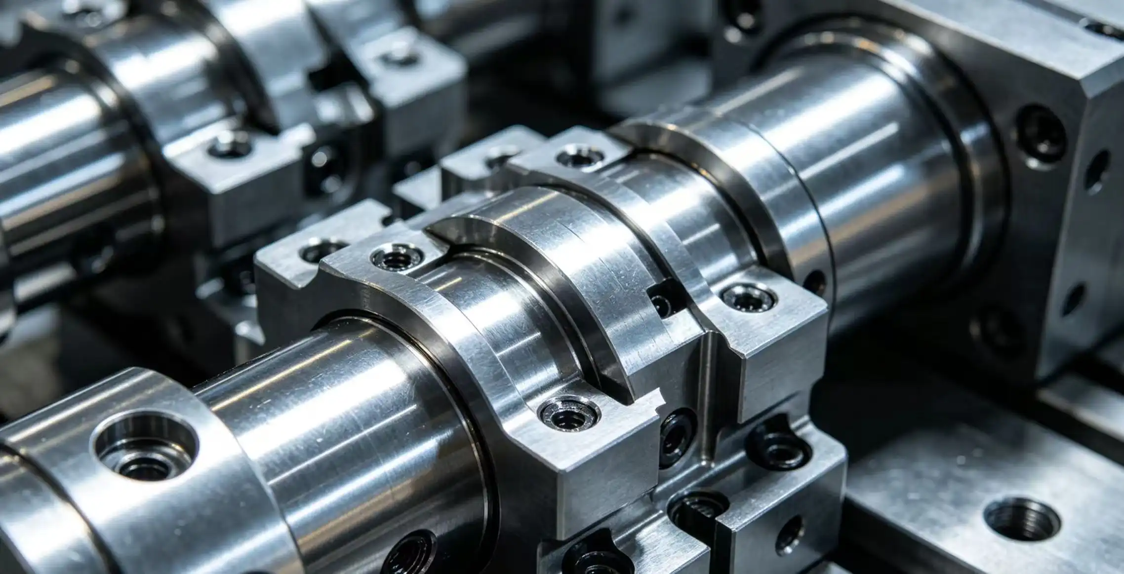
Choosing the Right Precision CNC Turning Partner for Photonic Components
Evaluating Manufacturing Capabilities
The first step in choosing reliable providers is to look at the equipment specs and quality systems. Look for coordinate measuring tools that can check geometric measurements and tolerances, especially the position, concentricity, and perpendicularity limits that are common in photonic housings. Video measurement devices can check optical surfaces without touching them, which is not possible with probe-style CMMs.
Material knowledge is what sets good shops apart from great ones. For thermal qualities, photonic uses often call for aluminum alloys. However, some parts need brass for electromagnetic shielding or stainless steel for places that are likely to rust. Aside from general "aluminum" labels, suppliers should show that they know how to read material certificates and understand the differences between 6061-T6 and 7075-T651 aluminum. Before cutting starts, XRF spectrometry checks the new material to make sure it meets the requirements.
Quality Control and Certification Standards
Tough checking rules keep measurements from changing between runs of production. Statistical process control tracking keeps an eye on important dimensions during runs and stops work before parts get too far out of range. Before mass production starts, standard conformance is set with first article inspection records that show full dimensional proof.
Basic quality management systems must be in place for ISO 9001 certification to be valid, but based on the end-use setting, photonic uses often need AS9100 aerospace standards or ISO 13485 medical device procedures. These approvals show that the processes are controlled, the equipment is calibrated, and there are tracking systems in place for parts that can fail in a big way.
The ability to treat the surface of an item makes it more useful. Type II anodizing adds an oxide layer that is 5–10 microns thick and resistant to rust. Type III hardcoat anodizing adds coats that are 30–50 microns thick and resistant to wear. It's important to know how to compensate for anodize thickness because providers have to machine pre-anodized dimensions smaller than needed to account for coating buildup. This is done to make sure that the final dimensions meet standards after finishing.
Communication and Service Breadth
Project timelines can be sped up with good expert communication. Before production starts, suppliers should look over the plans ahead of time to find any problems that might come up during production. When specs call for impossible tolerance combos or geometric controls that don't work together, experienced partners suggest changes to the design instead of moving forward with lower quality.
Before investing in production tools, prototyping services make sure that ideas work. Design-for-manufacturability processes that are done quickly help find problems early, when changes only cost a few hundred dollars instead of thousands. Customization freedom adapts to changing needs as photonic technologies improve, letting design changes be made in the middle of a project without having to go through long contract renegotiations.
Contractual and Sourcing Considerations
Quotes based on projects are used for prototypes, while deals based on quantities are used for production runs. Accurate planning is possible with clear separations between material, machining, testing, and finishing costs. Minimum order amounts should be in line with inventory plans. If the minimums are too high, capital will be stuck in extra parts, and if the batches are too small, the cost per unit will go up.
When you source from within your own country, you can communicate more quickly and get your products faster, but you usually have to pay more. International providers can save you money, but they make things more difficult when it comes to checking quality, protecting intellectual property, and coordinating supplies. For many projects, hybrid methods that include prototyping in the U.S. followed by qualified production overseas are the best way to combine speed and cost.
Lead time promises are important when a photonic module start has to happen by a certain date. Penalty terms that protect against late supplies need to be weighed against the ability of the provider to handle schedule risks. Reasonable gaps allow for unplanned delays in materials or equipment breakdowns that don't stop whole projects.
Future Trends: How Photonic Integration and Precision CNC Turning Will Co-Evolve
Emerging Photonic Technologies
Silicon photonics is the next big thing in integration. It makes optical parts using methods for making semiconductors that were originally used in electronics. Even though these chips have thousands of optical elements built into silicon plates, they still need to be protected from the world and kept cool with precision-machined packages. In heterogeneous integration, III-V compound semiconductors are combined with silicon platforms. This makes it possible for laser sources to be directly attached to silicon waveguides, which requires even tighter package tolerances.
With co-packaged optics, photonic chips are placed right next to processor dies, so there are no electrical connections between the chips. For this design to work, the optical and electrical parts have to be lined up on a nano scale. This means that mechanical support structures have to go into areas that were previously used by semiconductor lithography equipment.
Manufacturing Advances Enabling Complex Components
With thermal adjustment systems that change toolpaths based on machine temperature, ultra-high precision CNC turning centers can now repeat within a few microns. In traditional bearing designs, mechanical friction made it hard to tell where the bearings were positioned. Hydrostatic bearings get rid of that problem. These improvements make it possible to directly machine features that are close to optical production limits.
In hybrid production, tools use both adding and taking away parts to make things. Laser metal casting creates forms that are close to nets, which are then finished off by precision CNC turning to the final size. This mixture works well for small photonic housings with complicated cooling ducts inside, which can't be done with regular machining but need to be turned for optical interfaces.
Multi-material turning methods combine different types of metals into one part. Aluminum bases conduct heat well, and brass pieces that are machined into the base make the threads last longer. These hybrid systems cut down on the number of parts needed in photonic modules, which makes supply lines easier and increases reliability.
Strategic Procurement Recommendations
Procurement teams that look to the future build ties with suppliers instead of just doing business with them. When you have a collaborative development deal, you share design information earlier, which lets manufacturers weigh in on the idea stages, when changes are least expensive. By investing together in specialized tools or testing equipment, the supplier's skills are brought in line with the needs of the program.
Spreading out the risks in the supply chain lowers them as photonic operations get bigger. By qualifying more than one provider, you avoid having a single point of failure and keep the competition going, which leads to continuous growth. Partners are made sure to keep investing in tools and training to keep up with changes in technology through regular capability checks.
According to market predictions, the demand for photonic components will grow by 40% each year until 2030, when data center owners will have switched to new infrastructure. Early interaction with suppliers ensures production capacity before demand exceeds supply. Long-term deals lock in good prices and make sure that everyone gets their fair share when supply is low.
Conclusion
Photonic integration completely changes the structure of a data center by swapping electrical interconnects that are limited by bandwidth with optical paths that can handle terabit-scale performance. For this change to work, the parts must be precisely machined to keep the micron-level limits that allow light to pass through reliably. Precision CNC turning is the main method used to make the housings, joints, and alignment structures that these optical systems need. Successful deployments are distinguished from costly fails by choosing qualified manufacturing partners who know both the basics of cutting and the needs of photonic applications. Manufacturing precision needs will get stricter as silicon photonics and heterogeneous integration methods get better. This means that ties with suppliers will become strategic assets instead of just transactions.
FAQ
How does anodizing affect precision-turned aluminum photonic housings?
Oxide layers are formed during anodizing, which makes the part bigger. Five to ten microns are added by Type II normal anodizing, and thirty to fifty microns are added by Type III hardcoat methods. To make up for it, skilled machine shops reduce the sizes of the parts they machine so that the finished parts meet all the requirements. Threaded connections get too tight without this adjustment, and joining surfaces lose the space they need. Always say whether the measurements on a picture show a pre- or post-anodized state.
What tolerances can modern CNC turning realistically achieve for photonic components?
These days' multi-axis precision CNC turning centers keep their positions accurate to within ±0.0001 inches (±2.5 microns) during production runs. It is common for cylindrical objects to have roundness limits of 0.0002 inches. When normal turning is used, the surface finish can reach Ra 0.8μm. When diamond shaping is used, it can reach Ra 0.4μm. These features meet the needs of most fiber-optic connection bodies and optical housing uses without the need for extra work.
Why choose turning over milling for photonic component fabrication?
When you turn, the cutting tool stays in place against the spinning workpiece the whole time. This results in better surface finishes and concentricity than milling's irregular multi-point cutting. Photonic housings are mostly cylinder shapes, which are great for turning. Parts that are rotationally symmetric take less time to make and cost less to cut. Milling is only needed when the design has non-cylindrical parts like rectangular pockets or flat fixing surfaces.
Partner with Precision CNC Turning Manufacturers Who Understand Photonic Applications
BOEN Prototype has a lot of experience making high-tolerance parts for projects that involve optical systems and data infrastructure. Our precision CNC turning skills give photonic housings the micron-level accuracy they need, and they are backed up by CMM proof and strict geometric dimensioning inspection processes. We can make parts out of aluminum, brass, and stainless steel with finishes as fine as Ra 0.4μm to meet the needs of fiber-optic connections and laser module enclosures.
Our combined manufacturing platform does more than just turning. It also has CNC machining, rapid injection molding, and metal casting all under one roof. This lets us make full photonic assemblies without having to coordinate with multiple vendors. Our engineering team works together throughout the development process to make sure that the final product is as easy to make as possible, whether you need multiple prototypes to make sure the design is correct or large quantities to support data center deployments.
Get in touch with our technology experts at contact@boenrapid.com to talk about your needs for photonic components. We know the quality standards and delivery times your projects need because we are a precision CNC turning provider with experience in the aerospace, medical device, automotive, and electronics industries.
References
Cheng, Q., Bahadori, M., Glick, M., Rumley, S., & Bergman, K. (2018). Recent advances in optical technologies for data centers: a review. Optica, 5(11), 1354-1370.
Thomson, D., Zilkie, A., Bowers, J. E., Komljenovic, T., Reed, G. T., Vivien, L., & Fedeli, J. M. (2016). Roadmap on silicon photonics. Journal of Optics, 18(7), 073003.
Margalit, N., Xiang, C., Bowers, S. M., Bjorlin, A., Blum, R., & Bowers, J. E. (2021). Perspective on the future of silicon photonics and electronics. Applied Physics Letters, 118(22), 220501.
Stephens, M. P. (2019). Productivity and Reliability-Based Maintenance Management (2nd ed.). West Lafayette: Purdue University Press.
Klocke, F., & König, W. (2018). Manufacturing Processes 1: Cutting (9th ed.). Berlin: Springer-Verlag.
Wade, M. T., Shekhar, S., & Kumar, S. (2020). Energy-efficient photonic interconnects for computing systems. Proceedings of the IEEE, 108(5), 765-778.

How Can We Help?

Your Trusted Partner in Rapid Manufacturing.